Last time we looked at using the SWD interface of an STM32 ARM chip. This isn’t the only way we can interact with this device though. It also contains a serial interface on the bootloader than allows us to read and write to the flash memory. It’s nowhere near as powerful as the SWD interface.
This example is rather contrived. On a device this small, with pins around the edge, it is unlikely that SWD will be harder to access than serial. Both SWD and the serial bootloader can be “locked” by using RDP (Read Protection). However, we’ve seen many chips where different debug/programming interfaces have different security levels applied. Equally, serial ports are often more obvious or physically accessible than JTAG/SWD.
This is simply to teach some of the principles around reading datasheets, reading schematics, putting a device into another bootmode, and using different tools.
What is a bootloader?
A bootloader is generally the first code to run on a processor. It has the task of initialising hardware and executing the firmware. On complex systems, there will be a significant ROM bootloader permanently stored in the device to call a second bootloader.
On very simple ARM microcontrollers (like the Cortex-M0 we are using) there is no need for anything this complex. The processor looks to the second entry in the “vector table” (the reset vector), and executes the code at this address.
However, STM32 have a ROM bootloader stored in something called “system memory” (STMicroelectronics call it that, not sure why). Using pins and flash options, you can choose different boot modes:
- Execute from flash (normal operation)
- Execute from system memory (which we will look at)
- Execute from SRAM (sometimes used for programming)
The system memory on the STM32F030R8 allows use to use a serial interface to communicate with the device. Some other STM32s allow I2C or USB.
Datasheets Everywhere
With the STM32 range, there are four sets of documents of most interest to us:
- Product Specification (often just “the datasheet”) – this largely concerns the physical and electrical interfaces. The pinouts will be here, and in STM32 ones, the memory map is also here.
- Reference Manual – this contains detailed descriptions of the peripherals and registers inside the device.
- Programmer’s Manual – this contains detailed information about the instruction set of the processor.
- Application Notes – smaller documents concerning the implementation of specific functionality in a device
For the STM32 range, most or all documents are publicly available.
The nomenclature used and the information contained in various documents is totally inconsistent across the semiconductor industry.
Boot Modes
In the product specification, we can see reference to the “Boot Modes”. There is not very much information.
In the reference manual, detail is given on how to go into various boot modes. We want to go into “system memory”. There are two inputs to this function: nBOOT1 bit and BOOT0 pin.
By default, the device is booting from flash memory. The BOOT0 pin must therefore be pulled low.
nBOOT1 bit is “x” which means “don’t care”. We need to check what this is, and if we need to change it. Searching the reference manual for nBOOT1 shows us it is single bit in the option byte.
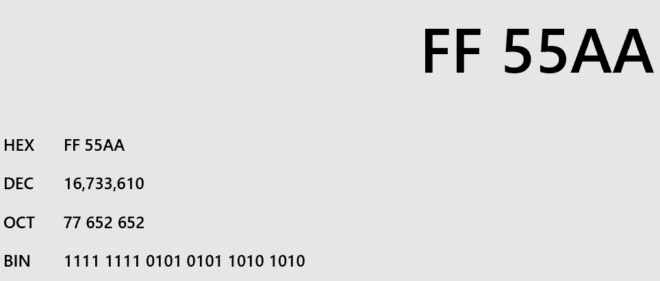
The default value is 0x00FF55AA – we need to work out what bit 20 is. If you work much with hex, it’s obvious, but it’s useful to be able to use a calculator to do this.
We can type the value into Windows calculator and see the binary value immediately.
Now, we could painfully count out the bits, but by pressing the little “dots” button, the window shows a convenient display.
Bit 20 – nBOOT1 – is set to 1 by default. This is what we want!
(0x00FF55AA clearly has bit 20 set as the byte it is in is 0xFF – all 1s)
Now we need to work out how to set pin BOOT 0.
For this we want to look back to the product specification.
It’s a clearly labelled pin – pin 60. Just a bit of advice – never assume that images in datasheets have searchable text! You might have to scan page after page.
We could use a multimeter to find where this pin goes, but it’s a development board – we have the schematic.
There’s a few things worth noting about schematics.
The two yellow boxes – U5A and U5B – both refer to U5 – the microcontroller. It’s just split into different parts to make the document easier to understand.
The pin numbers are not organised sequentially. Again, they are put into whatever order makes the document easier to understand.
The yellow diamond boxes mean that a signal (or group of signals) are jumping to another page.
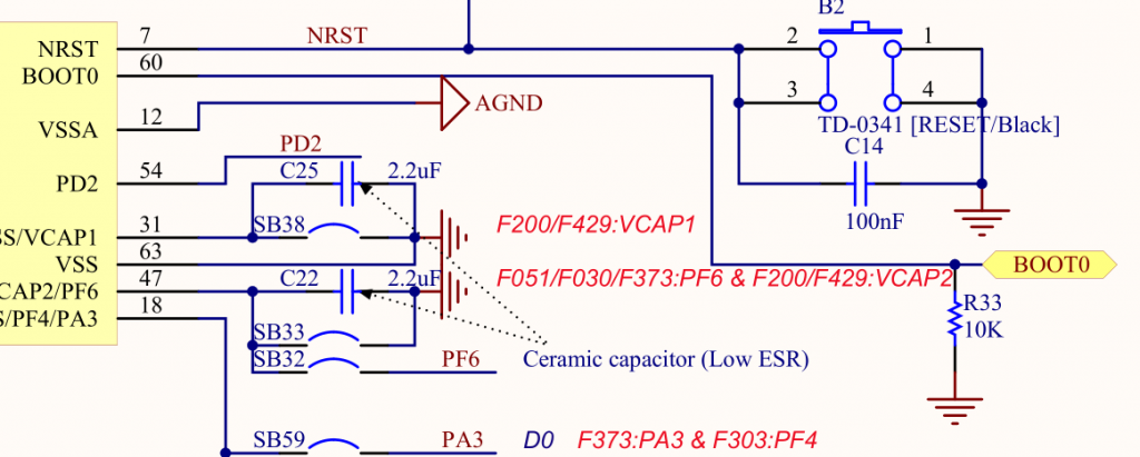
BOOT0 – pin 60 – can be seen on U5B. It then leads off to R33 – a 10K resistor. This is a “pull down” resistor – designed to hold the logic level at 0 unless the pin is connected directly to a high level.
Where does the BOOT0 signal go? It jumps to another page.
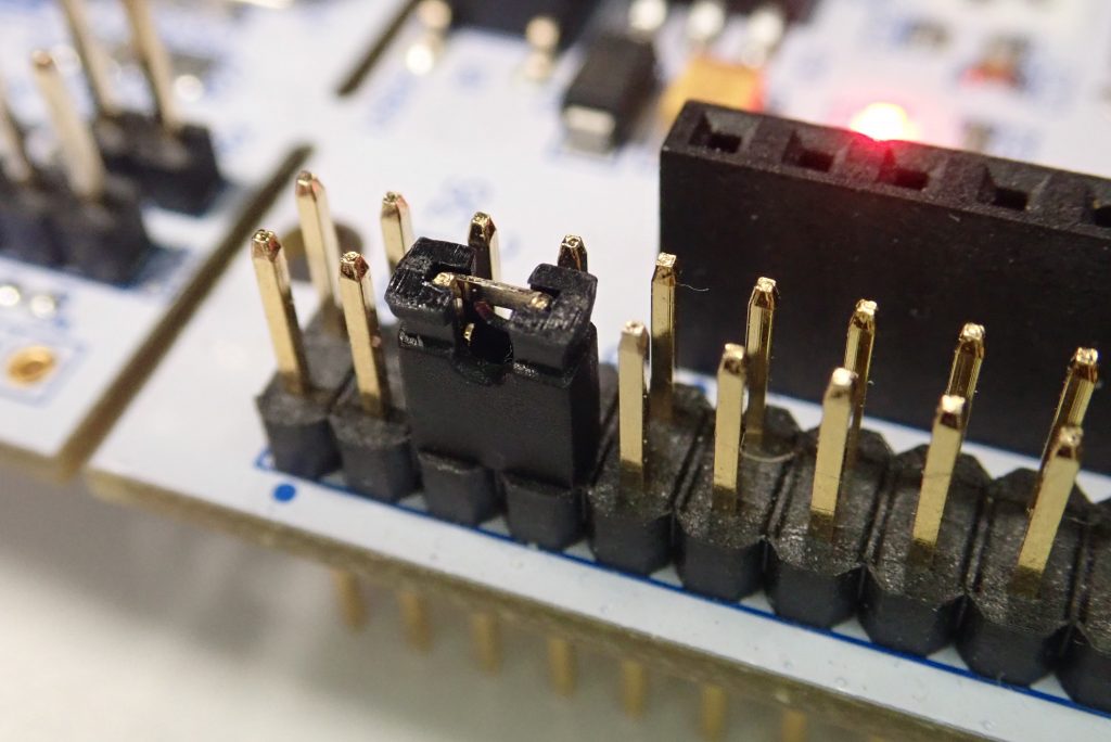
Pin 7 on connector CN7 – nice! All we need to do is connect this to a high logic level, and the device will enter the system memory. Conveniently, immediately above pin 7 – pin 5 is “VDD”, which is the supply voltage for the processor. We can use one of the spare jumpers from CN11 or CN12 (which are just holders for spare jumpers) to bridge the two.
This is easily tested – your board should be running the blinky LED code by default. Place the jumper on, and press the black reset button. The LED should no longer be blinking as the flash code won’t run.
Finding the UART
The product specification mentions that the bootloader can be accessed on pins PA14/PA15 or PA9/PA10. We want the most readily accessible ones.
Back to the schematic. PA14/15 are brought out on CN7 pins 15 and 17 – adjacent to each other.
Interacting with the bootloader
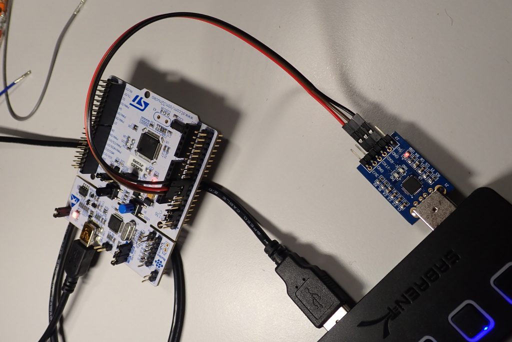
We have the device starting up in the bootloader, and we know which pins to connect to. Whilst the development board does have a built-in USB serial adapter, it is connected to USART2 on PA2/PA3. It’s not trivial to reconfigure the board, so we will use an external USB serial adapter.
Look back to the post on interacting with serial ports if you can’t remember how to use them. Remember that TX goes to RX and RX goes to TX.
The software we will be using is called stm32flash. Yes, it is SourceForge, and yes, SourceForge is somehow still alive. Download the latest release called “stm32flash-0.5.tar.gz“.
The following should be done to unpack, build, and install it:
tar -zxvf stm32flash-0.5.tar.gz
cd stm32flash
make
sudo make install
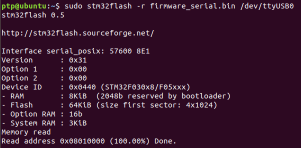
With the STM32 development board powered up, the jumper pulling BOOT0 high, and our serial adapter connected, you should then be able to run:
sudo stm32flash /dev/ttyUSB0
This will query the device for information. If it doesn’t work, try flipping TX and RX.
And now, using other commands, we can read and write the flash.
Conclusion
We’ve used a very similar trick on the LPC5460x series of chips, which can have SWD/JTAG disabled, but you can set the device into a USB boot mode that allows you to read the firmware back over USB. Always check the datasheets for the processor you are working with to uncover “hidden” functionality like this.







» Reading and writing firmware on an STM32 using the serial bootloader – Library Project: Epilogue
November 5, 2020 at 5:35pm[…] https://cybergibbons.com/hardware-hacking/reading-and-writing-firmware-on-an-stm32-using-the-serial-… […]